The Bernina 1130 we have is from 1986. There’s a motor driver board built with twelve op-amps and lots of resistors. Let’s figure out how it works using KiCad 8 for drawing.
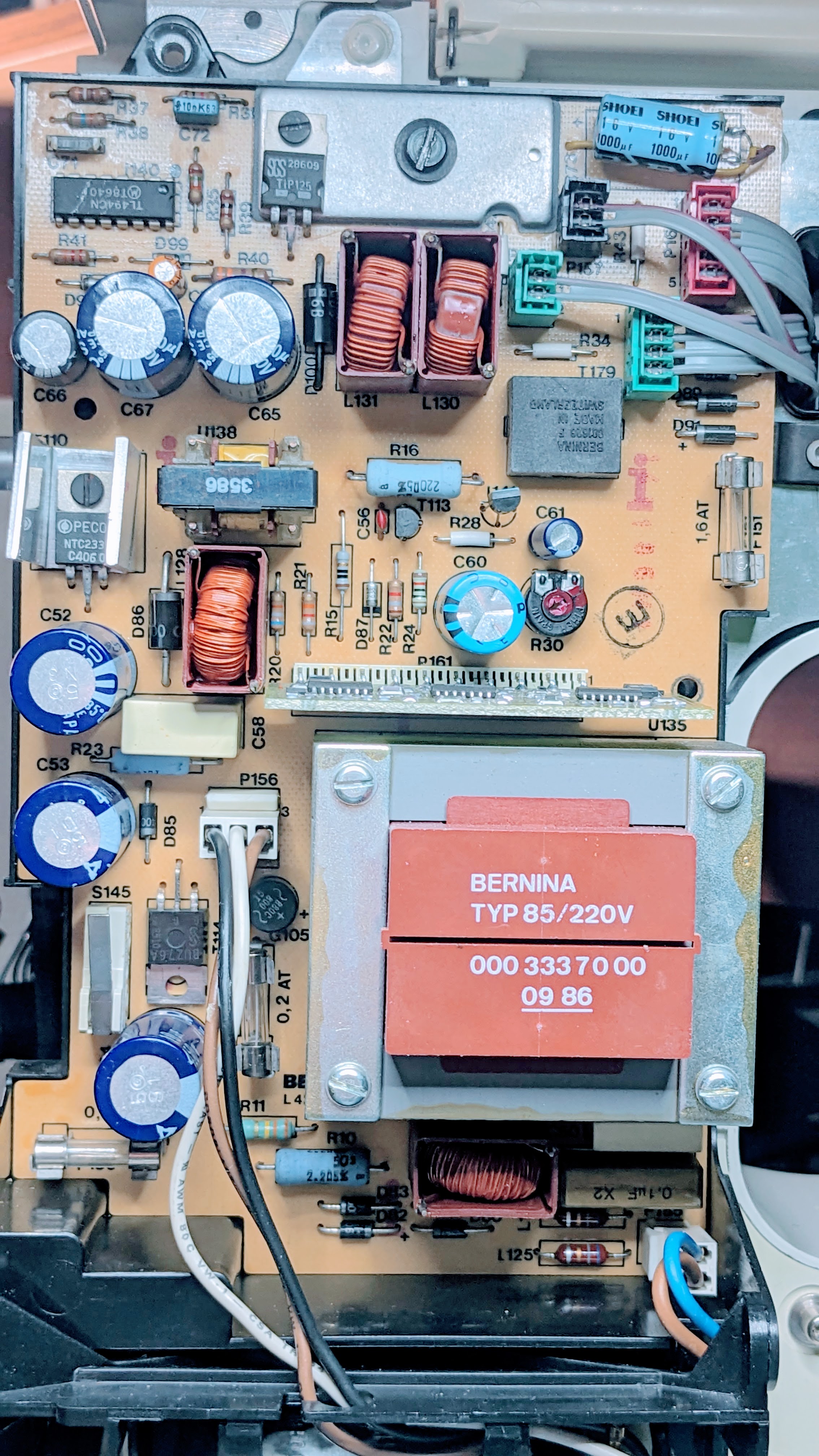
Oddly enough, there seems to be very little information on when the 1120/1130 models were sold. I found SyRep’s Sewing Machine Repair Resources, which has schematics of the L4200 power supply unit of the 1120/1130 machines, with date code from 1985. Perhaps that’s when they were introduced. A great resource!
However, there’s a daughter board that has the motor driver, sitting right above the transformer. I wanted to have a schematic for that too, because for some reason the R16 (large blue resistor) and T113 (right under R16) were getting really hot at idle. Since I had already fixed an 1120 with blown motor transistors, I figured this might be worth knowing more about.
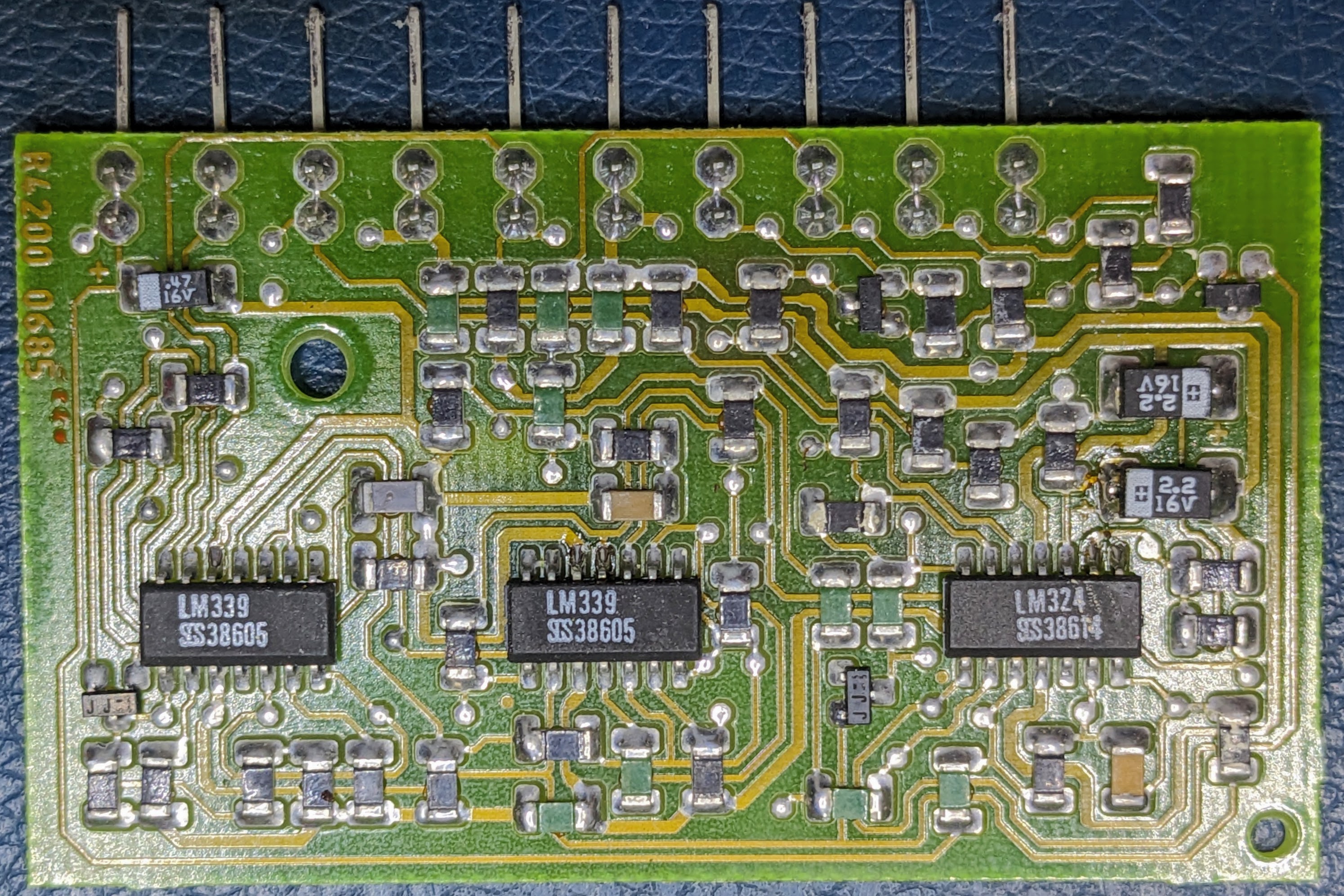
On the daughter board, called R4200, there are three op-amp packages on there, i.e. 12 in total. It’s surface mount components, which is cool, because the rest of the machine is through-hole.
Reverse Engineering With KiCad
It’s a single-sided board, so I took a photo and opened it in the KiCad PCB editor, after some manual rotation and perspective adjustment. I knew the pin header had a 0.2” pitch, so I could set the scale based on that. Next, I added footprints, including some guesswork on which footprints were used. And then traces, following the photo. There is no silkmask, so all referene designators are made up.
A big problem with using KiCad in reverse is that the workflow for importing from PCB to schematic is very spotty. There’s no way to generate nets. There’s the WireIt plugin, but that’s net-by-net, which is a pain. I ended up writing a plugin that does two things:
- It runs annotations, replacing e.g. the default reference designator R** with R1 and so on.
- It looks at actual copper overlap connections (something KiCad provides) and generates nets for them.

Thus we end up with a “routed” board that doesn’t have a schematic. It would be great to generate a schematic, but I didn’t feel like doing more coding for this, so I just manually added all components and then “updated from PCB” while linking using reference designators, not the component IDs. Eventually, I managed to get a connection between the PCB and schematic that yielded no diffs when trying to update either direction.
Another issue here is that because it’s a single-sided board, there are lots of jumpers. They are all green, and easy to tell apart from resistors, which is nice. KiCad PCB doesn’t deal well with footprints that have internal connections, and I didn’t want to include the jumpers in the schematic. I decided to start with adding the jumpers in the schematic, but then marked them as “board only” and made a special footprint for a 1206 SMD jumper where both pads had the same pin number. It still leaves one “unrouted” warning per jumper, but it’s easy enough to verify by hand.

So after all of that, what I had was a big hot mess of wires in a schematic. The next step was to do a bit of drawing by hand to try to rearrange the schematic. I started at the inputs and tried to figure out the layout that had the fewest crossing wires. The hand drawing worked pretty well, only screwing up a couple of relationships, as it turned out. It was essentially an exercise in creating a block diagram and grouping components by block. Because it’s a single-sided board, many components are spread out, and not close to where you’d normally draw them.
Getting all that into KiCad is a bit of a mess, though. Because there is no “rat’s nest” in Schema, you have to very carefully drag groups of components until you disentangle all of it. It’s pretty laborious, and I wish I had continued to write the PCB reverse engineering tool I started writing.

After two days of mucking around, it looked pretty good! I ran the PCB update to see if any changes looked wrong (i.e. if I had messed up connections without noticing.) It all looked pretty good, aside from those ten jumpers!
Here is the schematic as PDF. Of course, I take no responsibility for this being accurate, nor what you decide to do with mains voltage.
How It Works
The Motor Driver Interface
The motherboard of the 1130 has two output signals to, and one input singal from, the driver board.
- Output PWM for motor speed. It’s running at 20 Hz with a range of about 10-90% duty cycle.
- Output BRAKE engage. There is a clamp across the motor when it’s not in use, and that acts as a brake.
- Input RUN status. A binary signal of whether the motor is spinning or not. I assume this is used as a fault detector.
It’s a pretty simple interface. The brake signal has a slight delay, which might be because the Run feedback signal is low-pass filtered, and thus a bit slow.
These three signals go through optocouplers to the motherboard. The driver board runs at 12 V, but it’s running directly on rectified mains, and is driving a 300 V DC motor.
Motor Outputs and Quirks
There are only two outputs to the motor: OUTBRK and OUTDRV.
The OUTBRK signal goes to an N-FET (T114) on the L4200 that just clamps over the motor. It’s pretty straight-forward.
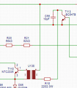
(from SyRep.no)
The OUTDRV signal goes to a transistor (T113) that fires up a gate-drive transformer (U138). This thing, though, is weird.
OUTDRV is active low, which means that it idles at high, which means it’s constantly feeding current through the gate driver transformer and its current limiting resistor (R16). What a silly design! The transformer acts as a short-circuit for DC, so this sewing machine literally has a built-in radiator. It looks to me like the driver board was made for driving a PNP/P-FET transistor, but they decided NPN+transformer is better. The resistor R16 is rated at 3W, and is the reason I got interested in the daughter board in the first place.
In the end, this is driving a DC motor, so they simply run a PWM signal output, but at 13.5 kHz. I.e. the whole driver board is essentially a frequency converter while maintaining the input duty cycle. There are also some feedback signals.
Motor Inputs
The VSENSE (which is called SENSE on SyRep) input monitors the motor windings. I don’t know if they check for back-EMF, or if this is just looking to see that the motor isn’t burned out. This is what’s used for the RUN signal, and is also the feedback signal for the control loop.
The other input seems to be ISENSE, using R23 as a shunt resistor. The SyRep L4200 schematic layout isn’t making it totally clear what the current path through the motor is, but seems likely. This signal is used to limit current, probably also helping if the motor is stuck.
The Potentiometer
There is a trim potentiometer (R30) on the L4200. I call it RIN. It’s tied to the PWM input pin, and I think it sets the minimum duty cycle/speed. (It sets the reference current used in the Q1-R10-R15 totem.) Could also be setting the maximum speed, if I got the polarity wrong. The PWM signal is active low, and since RIN is tied to +12V, it seems likely it has something to do with the minimum.
The 12 Op Amps
They use all of them. The U1 and U2 are LM339 and U3 is an LM324. The former is open-collector (KiCad uses a diamond and underline to signal that), while LM324 is push-pull. It’s interesting to note that even the push-pull is sometimes used as open-collector by adding a diode; see U3D.
One (U2C) or two (U2B) seem to be used as an inverter plus transistor, so I guess they had some to spare, and could save on a few transistors. I’m not great with analog electronics, so what follows is a cursory guess based on individual op-amp blocks.
- Aside from driving OUTBRK, the BRAKE input also seems to be used in two different output inhibits. Not disengaging the brake before driving the motor would burn the transistors, so I could understand that.
- There’s a low-pass filter for the PWM signal, before going in to an amplifier.
- That goes to an error integrator that integrates over the difference between the PWM signal and the motor VSENSE (which is also low-pass filtered.)
- The ISENSE goes through an amplifier and draws down the error if the current is too high.
- The PWM signal generation happens in two op-amps: one oscillator and one comparator. I couldn’t find very little precedent for this arrangement, but it seems they generate a “triangle” wave by tapping into the input side of a square wave generator. Pretty neat saving of an op-amp, since they know the PWM comparator will be a high impedance sink anyway.
- Once there is a PWM signal (but at a much higher frequency) it goes through an op-amp used as a pre-driver. Note that the OUTDRV is active high, so it’s the resistor that drives the power transistor, not the op-amp. This is why T113 and R16 on the L4200 is getting so hot at idle.
- Finally, the RUN output to the motherboard is simply checking if there is some movement on the motor. (The smoothed VSENSE is compared to a very small voltage from the main resistor ladder.) The emitter follower on the output is curious, since it’s only driving an opto-coupler at 300 µA. Surely this could be handled by the push-pull output of the LM324. Perhaps it too was meant to drive something else, like directly driving an indiator LED.
The Inhibits, Clamp and Shunt

I think the four op-amps I understand the least about are some of the left-most ones.
There is one output inhibit (U2A) that draws the error signal to zero if the BRAKE is engaged, if BRAKE is at least 4 V. This is the hard “don’t gas while braking.” Then there is another (U2D) that reduces the PWM input by adding a ground connection through R7. I don’t really see why they needed to pass this through U2B, which is just used as an inverter with open-collect output (hence why I called it a shunt.) It’s possible this is just used to discharge the input low-pass filter capacitor C5 to avoid start-up surprises.
The clamp (U2C) is also using the shunt. If the PWM input drops below a low threshold (2.4% or 0.3 V,) the clamp will help it reach zero faster.
Conclusion and Summary
To summarize my proposed signal names for the P151 connector on the L4200:
- PWM (output)
- RUN (input)
- BRAKE (output)
- RIN (not a good name; something about min or max speed)
- +12V (relative to GNDM)
- OUTDRV
- GNDM (separate ground for the motor and driver)
- ISENSE (motor current sensing)
- OUTBRK
- VSENSE (motor voltage sensing)
And this carries over to the P157:
- BRAKE (input)
- GND
- RUN (output)
- PWM (input)
As for the heat: the R16 and T113 components on the L4200 power supply get really hot because the R4200 board is probably being abused a bit. It doesn’t seem like a perfect fit either for the RUN signal output, or the OUTDRV driver. They knew this was a bad idea, but just beefed up the components. Since this is non-isolated from mains voltage, you’re not going to be touching these components anyway. (Unless you use an isolation transformer and at least pretend to know what you’re doing.)
But it is beautifully optimized.